

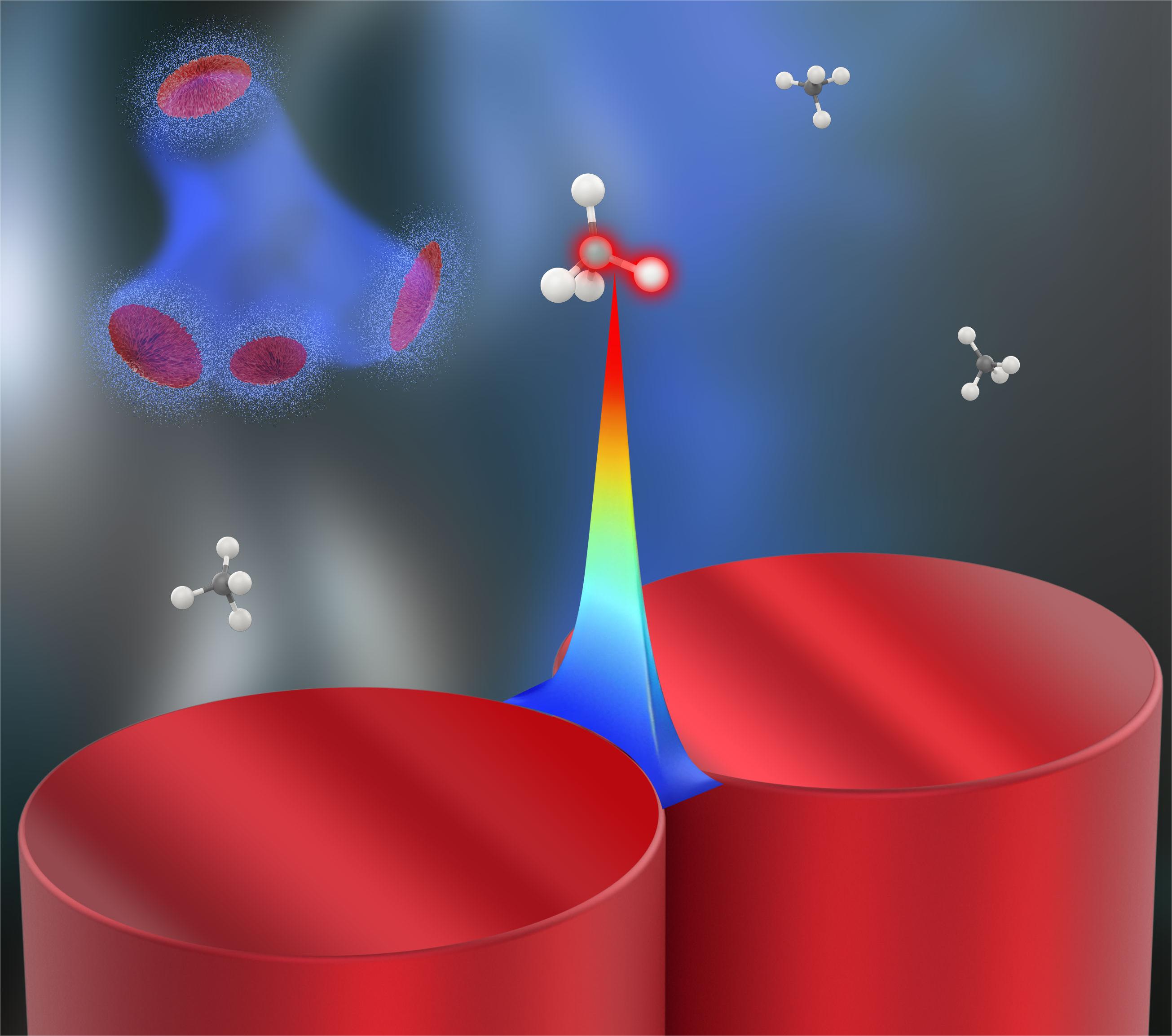
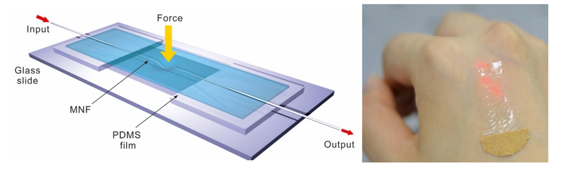
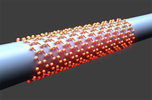
Insects have evolved highly optimized antennae with ultrasensitive tactile, auditory, and olfactory senses. Although imitating insect antennae offers a
promising route to achieving advanced sensing abilities, developing a micro-sized artificial antenna with ultrasensitive multisensory perception and
integrable with robotic systems remains challenging. Here, we report a bioinspired micro-optical antenna (MOA) comparable to biological antennae in both
architecture and functionality, leveraging an optical micro/nanofiber (MNF) encapsulated within a functionalized polymer film for both sensing and signal transmission.
By measuring the radiation or absorption of MNF-guided light induced by external stimuli, the MOA achieves ultrasensitive, fast-response, and low-power tactile,
auditory, and olfactory sensing. We further demonstrate a lightweight (~0.1 grams) MOA module mounted on a flapping-wing aerial robot and an insect-like ground robot,
enabling robotic multisensory perception and autonomous operation.
This work may pave the way for miniaturized versatile sensing systems that could be configured for a broad spectrum of technological applications.
— X. T. Tu et al.,
Sci. Adv. 11, eaec4252 (2025).
See also news and views in
前沿进展|Science Advances主页推荐:张磊/童利民团队联合李铁风团队发文报道一种超灵敏多感觉的微光学触角
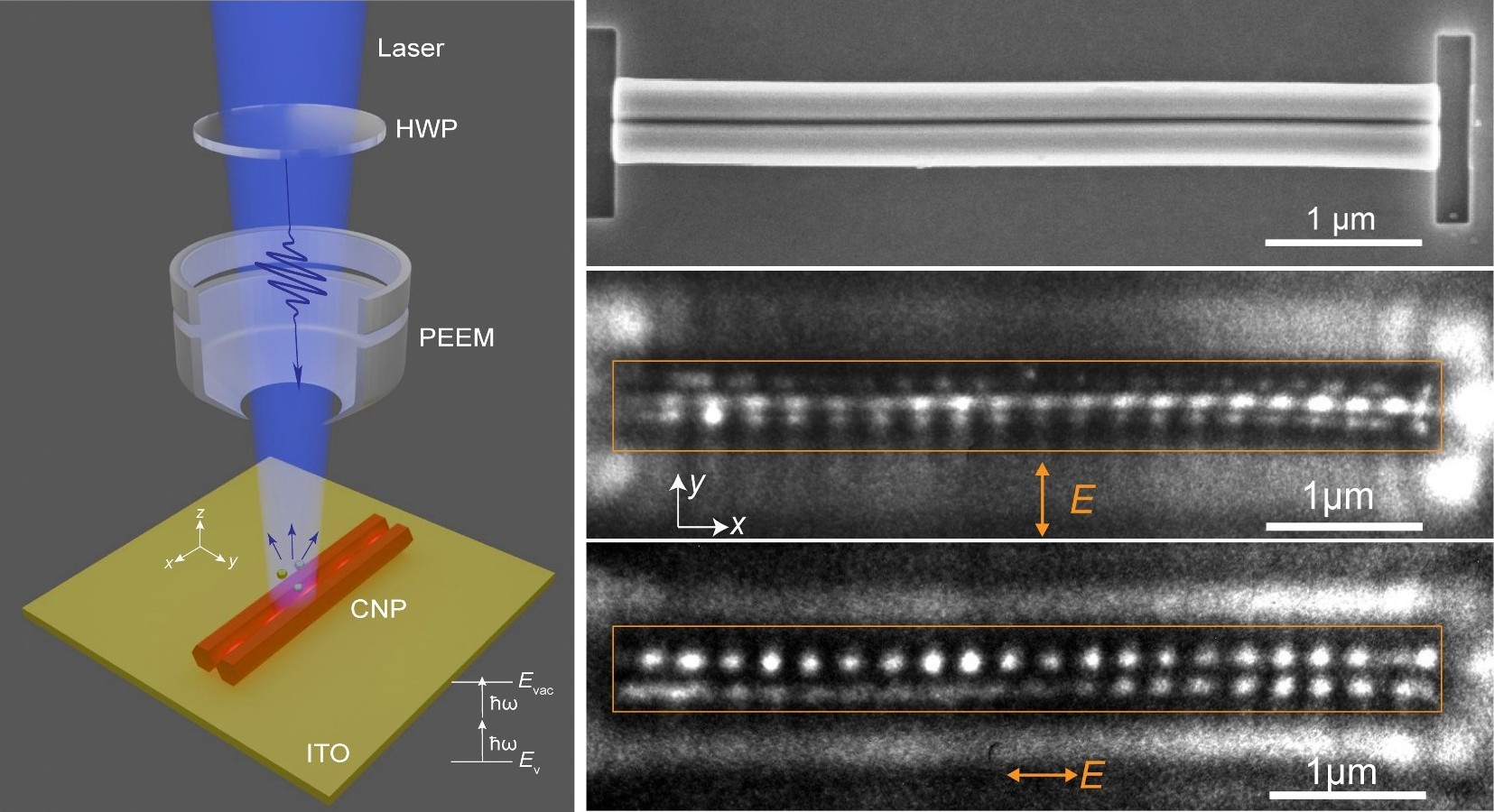
Ultra-confined optical fields are of great importance in fundamental optics and optical technologies.
The extreme field confinement in ultra-small nanostructures presents significant challenges in direct near-field characterization.
Conventional scanning near-field optical microscopy encounters difficulties in characterizing sub-10-nm confined light fields
due to significant disturbances of the optical field caused by the probe. Here, by employing a high spatial-resolved photoemission
electron microscopy (PEEM), we succeeded in imaging the ultra-confined near fields of a nanoslit mode in a coupled nanowire pair (CNP)
with weak disturbance for the first time and demonstrating a quasi-three-dimensional field distribution of the nanoslit mode.
We also show that, a PEEM image can identify fabrication defects that are influential to the confined field but are imperceptible to many other means.
These results open an opportunity for weak-disturbance characterization of ultra-confined optical near fields,
which is an essential step toward future optical devices or technology relying on ultra-confined light.
— L. Yang et al.,
Light-Sci. Appl. 14, 358 (2025).
See also news and views in
Light | 极弱扰动!极端约束光场的近场成像与表征
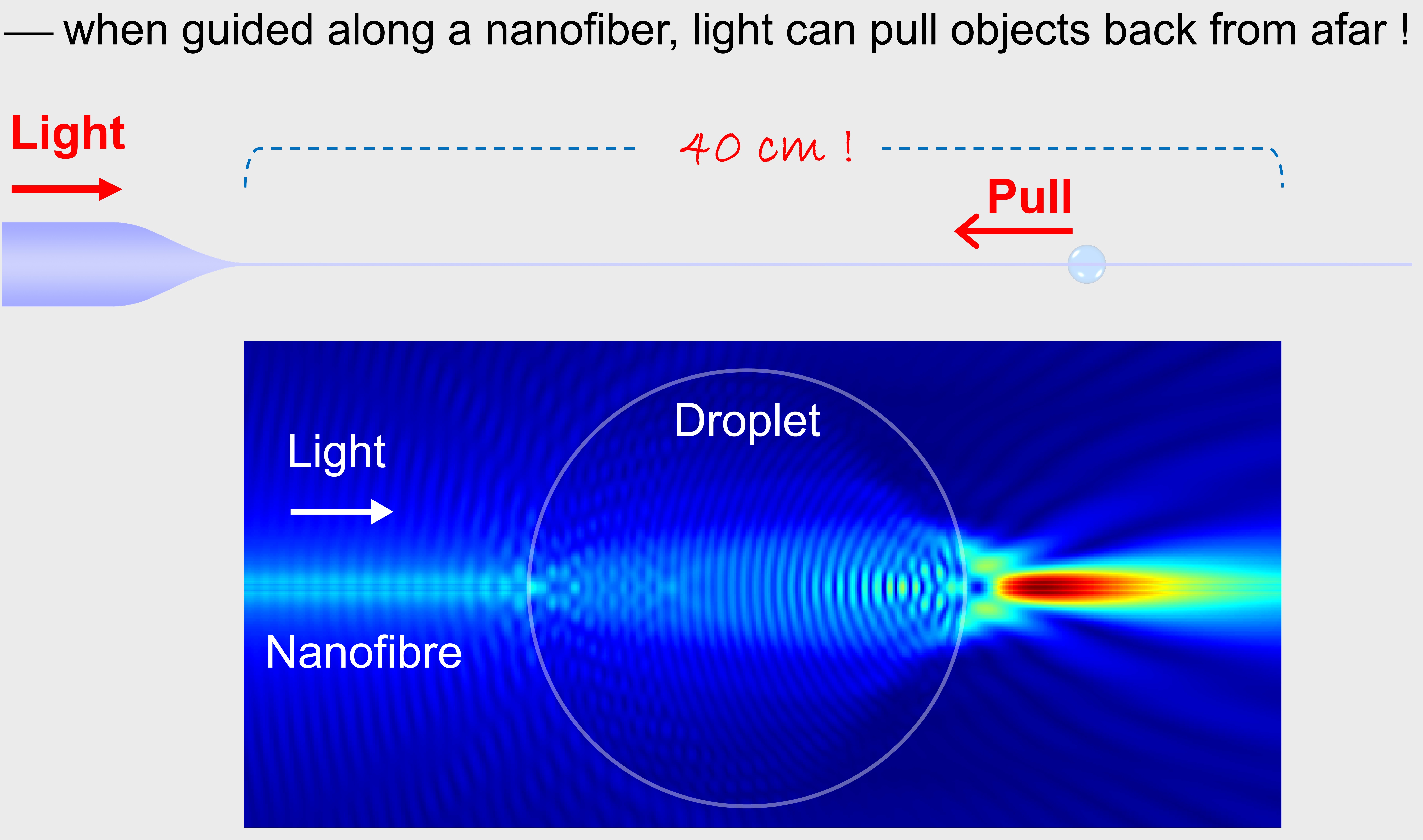
Single-beam optical pulling has attracted much attention owing to its counterintuitive nature,
interesting underlying physics and technical potential. Due to the difficulty in engineering wave vectors for
long-range optical pulling, to date, the available pulling range is less than 0.2 mm. Here we demonstrate a
40-cm-long optical pulling of a micro-droplet with an optical nanofibre based on the Minkowski-photon-momentum engineering of
its guided mode. Also, we have succeeded in vertically pulling up a micro-droplet against its own gravity. Such an ultra-long-range
optomechanical structure may offer a simple and effective platform for both scientific research and technological applications
from nanophotonics, optomechanics to biophotonics and optofluidics.
— J. B. Zhang et al.,
Nat. Commun. 16, 7424 (2025).
See also news and views in
前沿进展 | 郭欣、童利民团队在《Nature Communications》报道基于纳米光纤首次实现单光束超长程光拉力
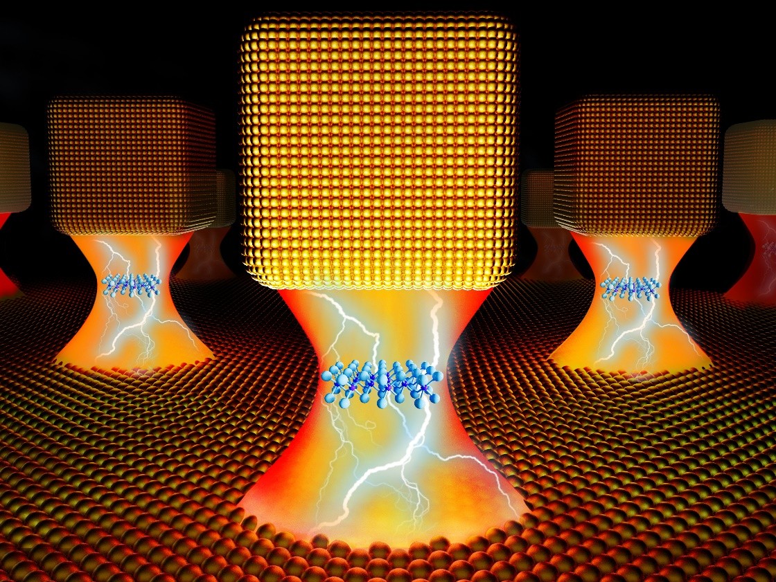
Enhancement and active control of light-matter interactions at the atomic scale is important for developing next-generation nanophotonic and quantum optical devices.
Here, we demonstrate electric control of excitonic strong coupling and electroluminescence (EL) by integrating a semiconductor monolayer into a nanometer gap of single
electrically driven nanocube-on-mirror plasmonic nanocavities, which provide unmatched optical and electrical conffnement. In particular, in a strongly coupled system of
nanocavity plasmons and tungsten diselenide (WSe2) excitons, an ultrastrong electric ffeld generated in the nanocavity gap enables reversible modulation of the Rabi splitting
between ~108 and 102 milli-electron volts with a bias of only 2.5 volts. In the quantum tunneling regime (realized by decreasing the gap size), by injection of carriers
into a nanocavity-i ntegrated tungsten disulffde (WS2) monolayer, spectrally tunable EL (controlled by the bias polarity) is achieved with a room-temperature quantum efffciency
reaching ~3.5%, showing an improvement of more than 103 times over previous works.
— J. S. Zheng et al.,
Sci. Adv. 11, eadt9808 (2025).
See also news and views in
前沿进展 | 王攀、童利民团队在《Science Advances》发文报道光电融合等离激元纳腔
Small organic molecules are essential building blocks of our universe, from cosmic dust to planetary surfaces to life.
Compared to their well-known gaseous and liquid forms that have been extensively studied, small organic molecules in
the form of ice at low temperatures receive much less attention. Here, we show that supercooled small-molecule droplets
can be drawn into highly uniform amorphous ice microfibers with lengths up to 5 cm and diameters down to 200 nm. In the
experimental test, these fiber-like ices manifest excellent mechanical flexibilities with elastic strain up to 3.3%.
Meanwhile, they can guide light with loss down to 0.025 dB/cm that approaches the material absorption limit and offer
high optical nonlinearity for low-threshold supercontinuum generation. Notable temperature-dependent Young’s modulus
and icing-induced refractive-index increase are also found. These results may open a promising category of
low-temperature materials for both scientific research and technological applications.
— B. W. Cui et al.,
Sci. Adv. 11, eads2538 (2025).
See also news and views in
前沿进展 | 童利民、郭欣研究团队在《Science Advances》发文报道有机小分子冰微纳光纤
Colloidal semiconductor nanocrystals are promising candidates for quantum light sources, yet their application has been impeded by photoluminescence instability due to blinking and spectral diffusion.
This study introduces a new category of cube-shaped CdSe/ CdS core/shell nanocrystals with exceptionally stable photoluminescence characteristics. Under continuous excitation, the emissive quantum
state remained consistent without alterations of the charge state for 4000 s, and the average photon energy variation stayed within the bounds of spectral resolution throughout this extended duration.
Systematic examination of single-nanocrystal photoluminescence, upon variation of the core and shell dimensions, revealed that a thicker CdS shell and increased core edge length significantly curtail spectral diffusion,
considering that the nanocrystals possess well-controlled CdSe−CdS and facet−ligand interfaces. This study advances the optimization of colloidal semiconductor nanocrystals as high-performance quantum light sources.
— Y. Z. Ye et al.,
Nano Lett. 24, 2712-2718 (2024).
Highly sensitive and compact microforce sensors with piconewton-level resolution are essential in various fields. However, these sensors face the challenge of delicate fabrication, expensive instruments,
and complicated signal processing. Here, we report an ultrasensitive microforce sensor with a nanonewton-scale working range and piconewton-level resolution (picobalance) using a 500 nm diameter U-shaped
silica optical nanofiber (ONF) as the cantilever beam and a gold microflake as the sample tray. The ONF can detect its deflection upon microforce by monitoring the change of its transmittance, making it a
self-detection picobalance with a linear response to microforce in the range of 0–11.2 nN based on theoretical calculation. Benefiting from the extremely low spring constant of the ONF (e.g., 0.15 mN/m),
the picobalance achieves a force resolution of 3.3 pN in an experiment measuring the radiation pressure. As proof-of-concept demonstrations, measuring nanogram-level microparticles and radiation pressure are
realized. We believe that this easy-to-use picobalance has great potential for biological sensing, biomechanical research, and environmental monitoring.
— W. Yu et al.,
ACS Photonics 11, 2316−2323 (2024).
As the fiber diameter decreases to the subwavelength scale, optical micro/nanofiber (MNF) exhibits fascinating optical and mechanical properties.
Over the past two decades, optical MNFs have been emerging as a miniaturized fiber-optic platform for both scientific research and technological
applications. In this paper, we aim to provide a comprehensive overview of the representative advances in optical MNFs in recent years. Starting from
the basic structures and fabrication techniques of optical MNFs, we highlight linear and nonlinear optical and mechanical properties of the MNFs.
Then, we introduce typical applications of optical MNFs from near-field optics, passive optical components, optical sensors, and optomechanics to fiber lasers and atom optics.
Finally, we provide an outlook into future challenges and opportunities.
— J. B. Zhang et al.,
Photon. Insights 3, R02 (2024).
See also news and views in
1、中国激光杂志社——童利民/郭欣教授:微纳光纤——光与纳米世界的桥梁
2、Story Video——浙江大学童利民教授、郭欣教授团队深入剖析了微纳光纤的历史沿革与演进轨迹
3、Photonics Insights直播专场 | 童利民教授:微纳光纤——从玻璃细丝到纳米波导
4、Commentary——Michael Sumetsky, “Optical micro/nanofibers: achievements and future directions,” Photon. Insights 3, C03 (2024)
Two-dimensional single crystal metals, in which the behavior of highly confined optical modes is intertwined with quantum phenomena, are highly sought after for next-generation technologies.
Here, we report large area (>104 μm2), single crystal two-dimensional gold flakes (2DGFs) with thicknesses down to a single nanometer level, employing an atomic-level precision chemical etching approach.
The decrease of the thickness down to such scales leads to the quantization of the electronic states, endowing 2DGFs with quantum-confinement-augmented optical nonlinearity, particularly leading to more than
two orders of magnitude enhancement in harmonic generation compared with their thick polycrystalline counterparts. The nanometer-scale thickness and single crystal quality makes 2DGFs a promising platform for realizing
plasmonic nanostructures with nanoscale optical confinement. This is demonstrated by patterning 2DGFs into nanoribbon arrays, exhibiting strongly confined near infrared plasmonic resonances with high quality factors.
The developed 2DGFs provide an emerging platform for nanophotonic research and open up opportunities for applications in ultrathin plasmonic, optoelectronic and quantum devices.
— C. X. Y. Pan et al.,
Nature Commun. 15, 2840 (2024).
Water ice, one of the most ubiquitous and important solids on the earth’s surface, exhibits excellent optical properties.
Here we demonstrate ice microsphere optical cavities and explore their resonant characteristics for the first time.
Whispering gallery modes within the ice microspheres are excited in a broad spectral range from near-ultraviolet to near-infrared.
This work provides a promising platform for exploring ice optics on the microscale.
— X. Z. Li et al.,
Adv. Opt. Mater. 12, 2302609 (2024).
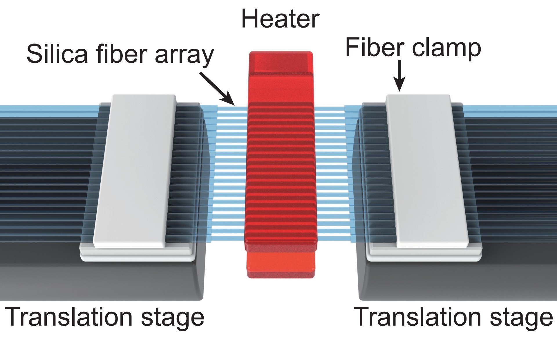
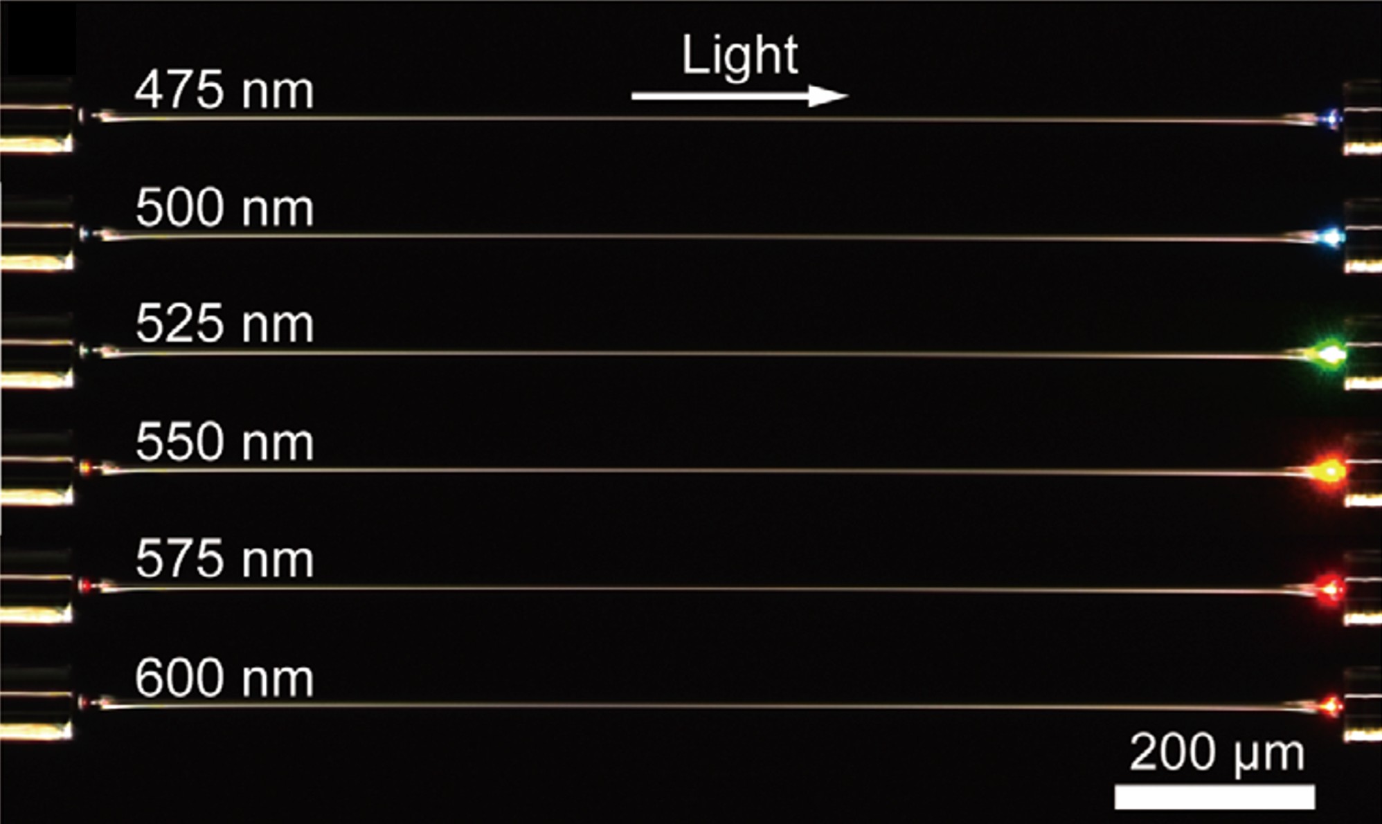
Optical micro/nanofibers (MNFs) taper-drawn from silica fibers possess intriguing optical and mechanical properties.
Recently, MNF array or MNFs with identical geometries have been attracting more and more attention, however, current
fabrication technique can draw only one MNF at a time, with a low drawing speed (typically 0.1 mm/s) and a complicated
process for high-precision control, making it inefficient in fabricating multiple MNFs.
Here, we propose a parallel-fabrication approach to simultaneously drawing multiple (up to 20) MNFs with almost identical geometries.
For fiber diameter larger than 500 nm, measured optical transmittances of all as-drawn MNFs exceed 96.7% at 1550-nm wavelength,
with a diameter deviation within 5%. Our results pave a way towards high-yield fabrication of MNFs that may find applications from MNF-based optical sensors,
optical manipulation to fiber-to-chip interconnection.
— H. B. Fang et al.,
Light-Adv. Manuf. 5, 20 (2024).
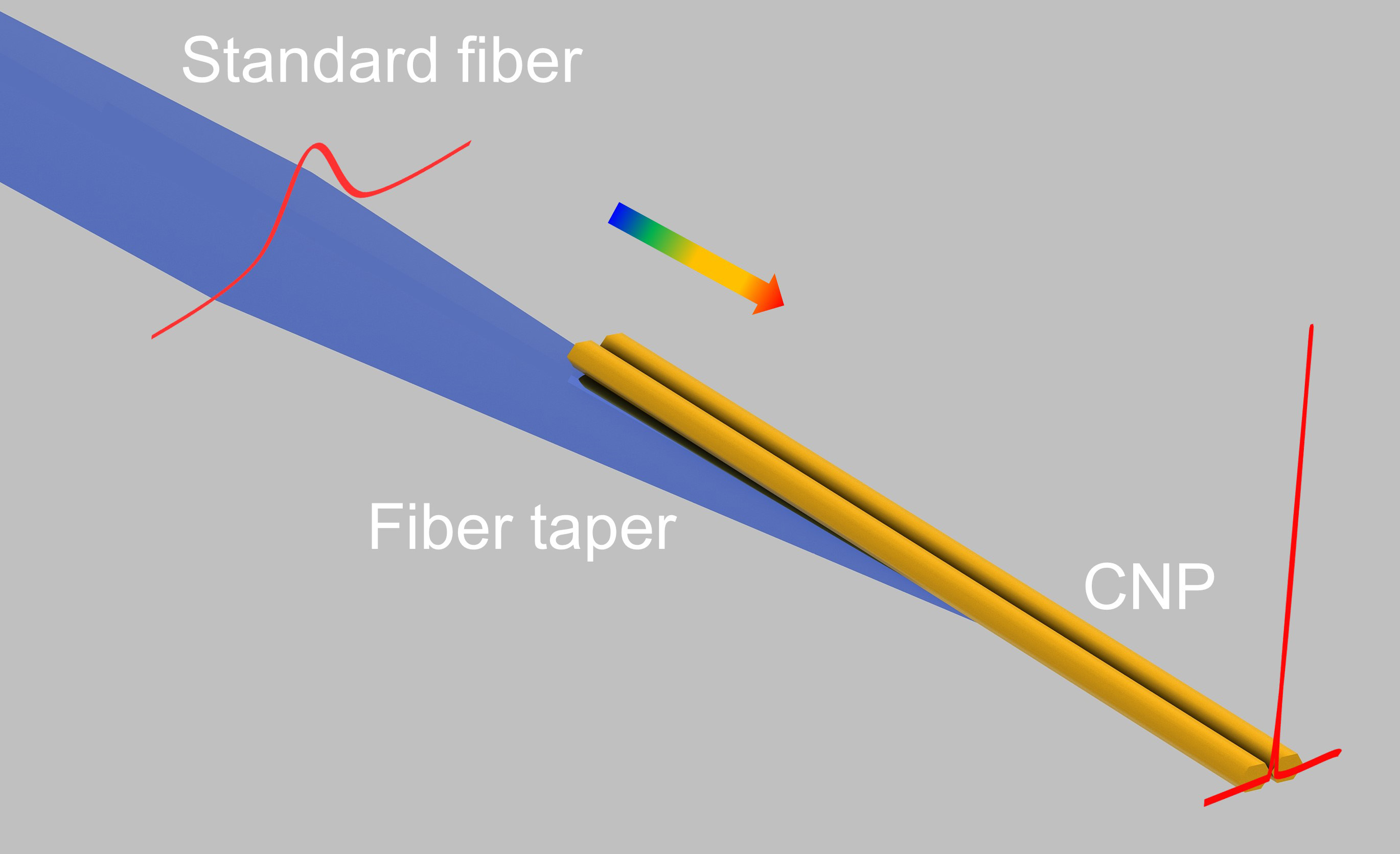
We propose to generate a sub-nanometer-confined optical field in a nanoslit waveguiding mode in a coupled nanowire pair
(CNP). We show that, when a conventional waveguide mode with a proper polarization is evanescently coupled into a properly
designed CNP with a central nanoslit, it can be efficiently channeled into a high-purity nanoslit mode within a waveguiding
length <10 μm. The CNP can be either freestanding or on-chip by using a tapered fiber or planar waveguide for input-coupling,
with a coupling efficiency up to 95%. Within the slit region, the output diffraction-limited nanoslit mode offers an extremely
confined optical field (∼0.3 nm × 3.3 nm) with a peak-to-background ratio higher than 25 dB and can be operated within a 200-nm
bandwidth. The group velocity dispersion of the nanoslit mode for ultrafast pulsed operation is also briefly investigated.
Compared with the previous lasing configuration, the waveguiding scheme demonstrated here is not only simple and straightforward
in structural design but is also much flexible and versatile in operation. Therefore, the waveguiding scheme we show here
may offer an efficient and flexible platform for exploring light–matter interactions beyond the nanometer scale, and developing
optical technologies ranging from superresolution nanoscopy and atom/molecule manipulation to ultra-sensitivity detection.
— L. Yang et al.,
Adv. Photonics 5, 046003 (2023).
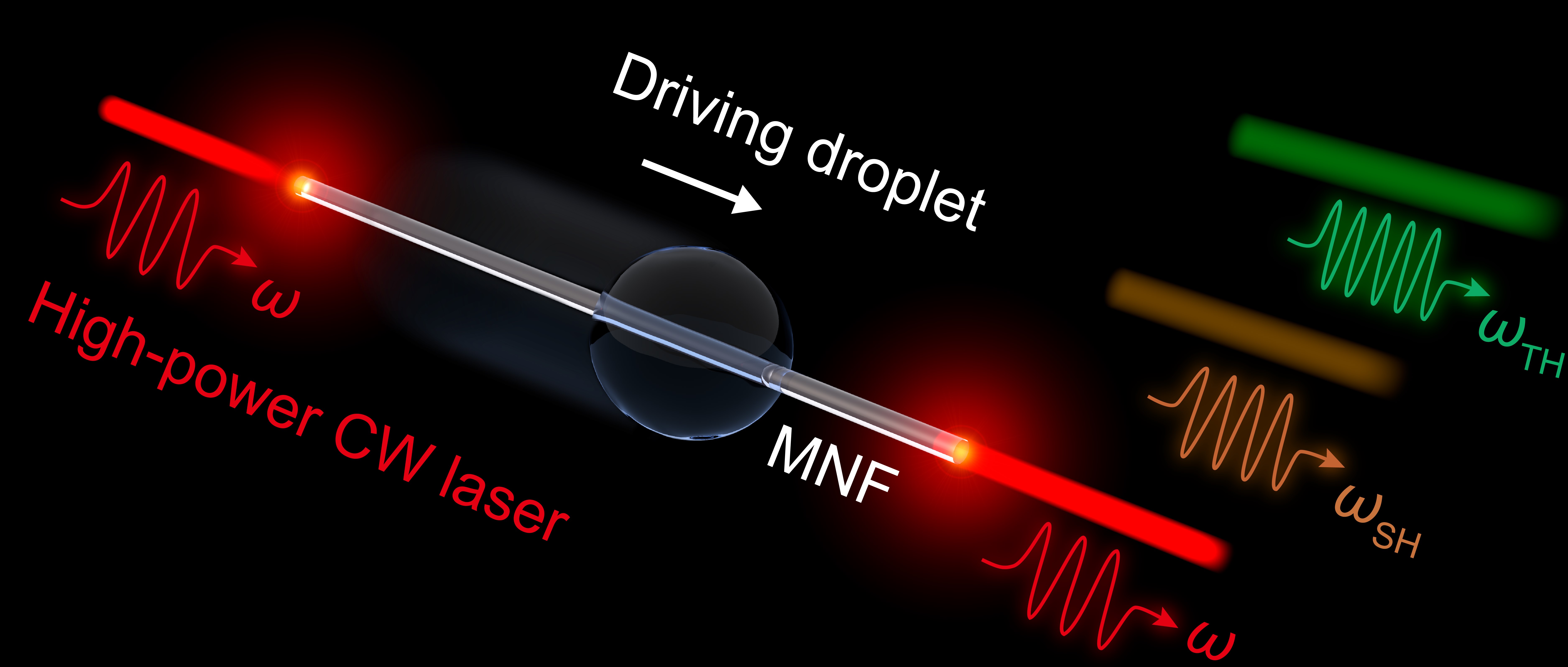
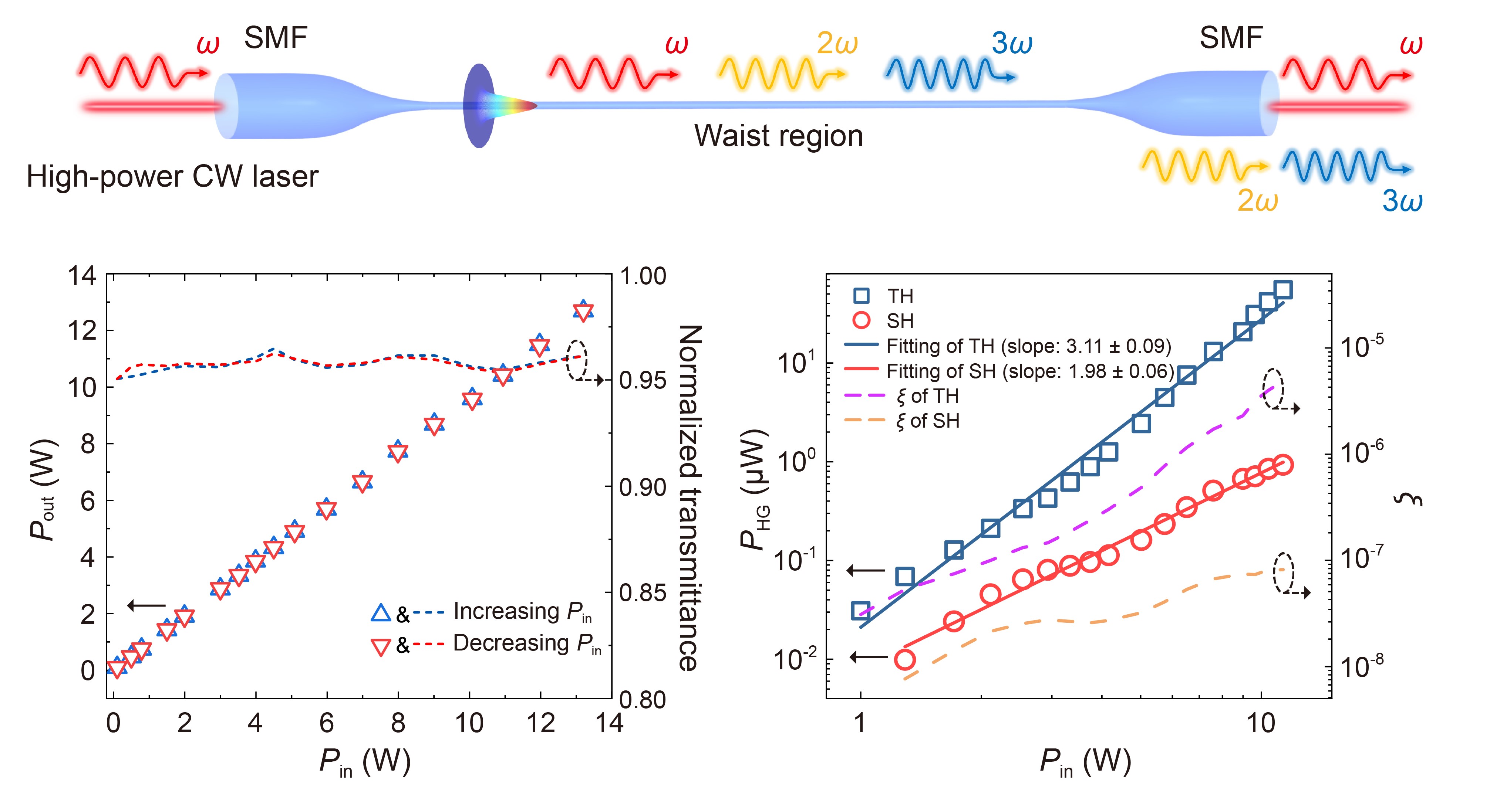
As miniature fibre-optic platforms, micro/nanofibres (MNFs) taper-drawn from silica fibres have been widely studied for
applications from optical sensing, nonlinear optics to optomechanics and atom optics. While continuous-wave (CW) optical
waveguiding is frequently adopted, so far almost all MNFs are operated in low-power region (e.g.,< 0.1 W). Here, we
demonstrate high-power low-loss CW optical waveguiding in MNFs around 1550-nm wavelength. We show that a pristine MNF,
even with a diameter down to 410 nm, can waveguide an optical power higher than 10 W, which is about 30 times higher than
demonstrated previously. Also, we predict an optical damage threshold of 70 W. In high-power CW waveguiding MNFs, we
demonstrate high-speed optomechanical driving of microparticles in air, and second harmonic generation efficiency higher than those pumped by short pulses.
Our results may pave a way towards high-power MNF optics, for both scientific research and technological applications.
— J. B. Zhang et al.,
Light-Sci. Appl. 12, 89 (2023).
An optical field with sub-nm confinement is essential for exploring atomic- or molecular-level light-matter interaction.While such
fields demonstrated so far have typically point-like cross-sections, an optical field having a higher-dimensional cross-section may
offer higher flexibility and/or efficiency in applications. Here, we propose generating a nanoscale blade-like optical field in
a coupled nanofiber pair (CNP) with a 1-nm-width central slit. Based on a strong mode coupling-enabled slit waveguide mode, a
sub-nm-thickness blade-like optical field can be generated with a cross-section down to ∼0.28 nm × 38 nm at 1550 nm wavelength
(i.e., a thickness of ∼λ0∕5000) and a peak-to-background intensity ratio higher than 20 dB. The slit waveguide mode of the CNP
can be launched from one of the two nanofibers that are connected to a standard optical fiber via an adiabatical fiber taper,
in which a fundamental waveguide mode of the fiber can be converted into a high-purity slit mode with high efficiency (>98%) within
a CNP length of less than 10 μm at 1550 nm wavelength. The wavelength-dependent behaviors and group velocity dispersion in mode
converting processes are also investigated, showing that such a CNP-based design is also suitable for broadband and ultrafast
pulsed operation. Our results may open up new opportunities for studying light-matter interaction down to the sub-nm scale, as
well as for exploring ultra-high-resolution optical technology ranging from super-resolution nanoscopy to chemical bond manipulation.
— Y. X. Yang et al.,
Photonics Res. 12, 154-162 (2024).
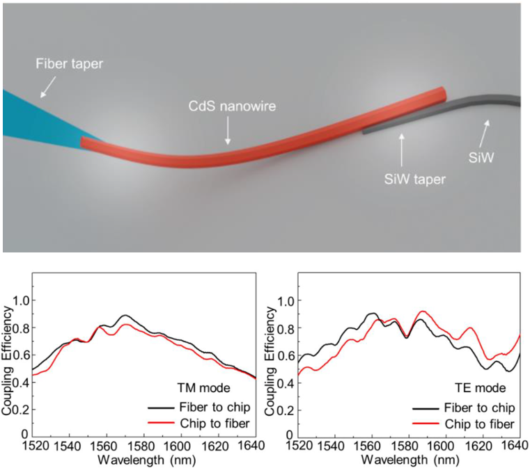
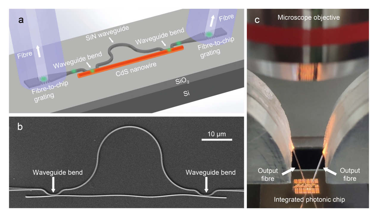
An efficient fiber-to-chip interface via an intermediated CdS nanowire is demonstrated. The fiber mode is firstly squeezed
through a fiber taper drawn at the end of a single-mode fiber, then evanescently coupled into an intermediated CdS nanowire
with a longitudinally tapering profile, and finally coupled into an on-chip silicon waveguide (SiW) via a waveguide taper
fabricated on it. Since the fiber-nanowire-SiW cascade structure is designed to match effective indices in each coupling
area, such a fiber-to-chip interface ensures a bidirectional coupling efficiency up to 90% and a 3-dB bandwidth over 100
nm in experiments. The difference of coupling efficiencies between the TM or TE modes is less than 0.5 dB in the spectral
range of 1545–1635 nm. The footprint of the on-chip coupling structure is about 10 µm in size. The results may provide a
compact, efficient, and versatile fiber-to-chip interface in applications including optical interconnects, coherent
communication, and quantum optical circuitry.
— Y. Y. Jin et al.,
Laser Photon. Rev. 17, 2200919 (2023).
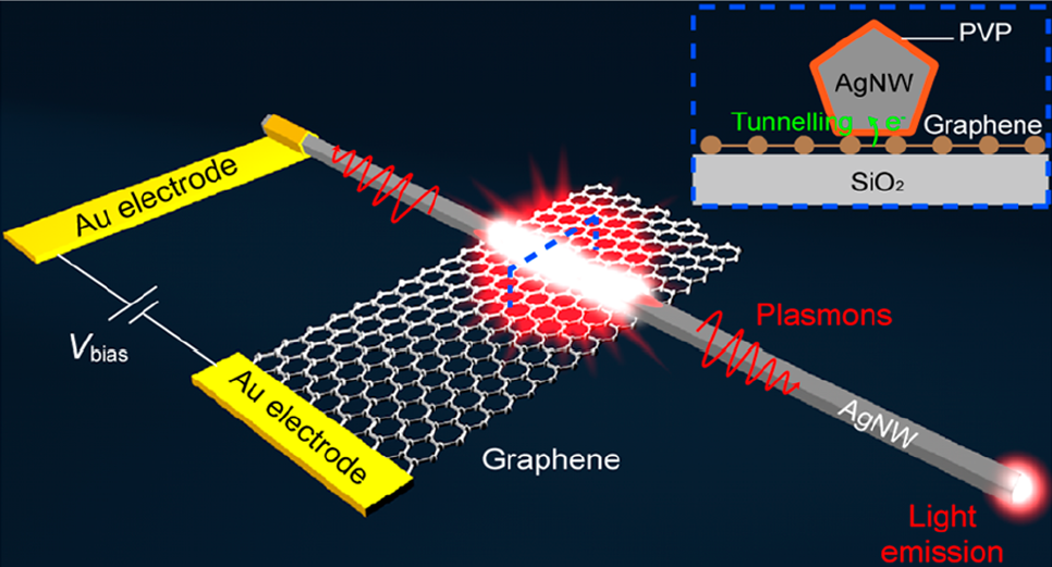
Ultrafast interfacing of electrical and optical signals at the nanoscale is highly desired for on-chip applications including
optical interconnects and data processing devices. Here, we break through the limitation of low-efficiency waveguided output of
inelastic tunneling-based light sources by developing waveguide-integrated metal−insulator−graphene tunnel junctions (MIG-TJs)
based on an organic layer-coated silver nanowire (AgNW) interfaced with graphene. The use of graphene instead of one of the metal
electrodes of conventional tunnel junctions not only eliminates the highly lossy MIM modes and therefore ensures efficient delivery
of the IET-excited optical signal to the edge of the tunnel junction where it can be extracted but also offers a small mode mismatch
between the tunnel junction region and the plasmonic nanowire waveguide, which enables efficient coupling (∼70%) of the optical
signal from the edge of the junction to the output AgNW waveguide. Furthermore, we demonstrate the coupling of the AgNW-integrated
tunnel junction with a low-loss semiconductor nanowire waveguide, thus realizing efficient outcoupling of the IET-excited optical
signal to both highly integrated plasmonic and low-loss photonic channels. Finally, as a proof of principle, a direct electrical
modulation of the outputted optical signal has been also demonstrated.
— L. F. Liu et al.,
Nano Lett. 23, 3731−3738 (2023).
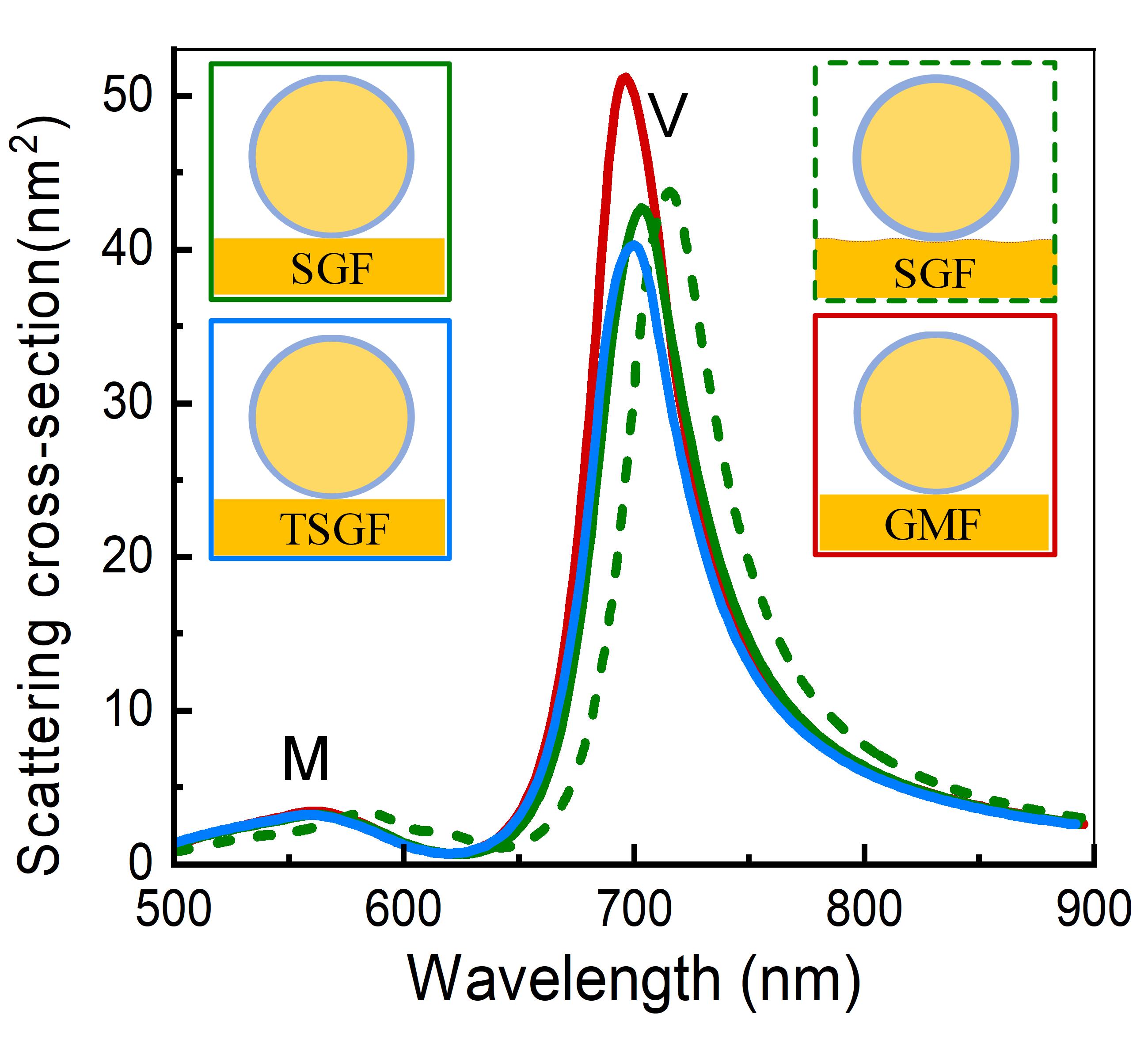
As an essential part of nanoparticle-on-mirror (NPoM) plasmonic nanocavities, metal mirrors play an important role not
only in determining the optical response of the nanocavities but also their performance in applications. In this work,
we experimentally study the effect of mirror quality on the optical response of NPoM nanocavities including nanosphere-on-mirror
(NSoM) and nanocube-on-mirror (NCoM) designs. Polycrystalline sputtered gold films (SGFs), template-stripped gold films (TSGFs)
and single-crystalline gold microflakes (GMFs) were investigated and compared. Due to the great improvement in the surface
roughness that can minimize fluctuations in the gap morphology, NSoM and NCoM nanocavities formed on smooth TSGFs and GMFs
have a better cavity-to-cavity homogeneity in the scattering spectrum than those formed on comparably rougher SGFs. In
addition, there is an obvious change in the spectral positions of the resonance modes of NSoM and NCoM nanocavities formed
on different gold films due to the variation in dielectric functions and surface quality of the gold films, which is reproduced
very well by theoretical calculations based on measured dielectric functions of the gold films. Moreover, due to the reduction
in electron scattering losses from SGF to TSGF and GMF, an increase in the quality factors and scattering intensities of the resonance
modes was observed for nanocavities formed on the corresponding films.
— Z. X. Wang et al.,
Adv. Opt. Mater. 11, 2201914 (2023).
As miniature fibre-optic platforms, micro/nanofibres (MNFs) taper-drawn from silica fibres have been widely
studied for applications from optical sensing, nonlinear optics to optomechanics and atom optics. While
continuous-wave (CW) optical waveguiding is frequently adopted, so far almost all MNFs are operated in low-power
region (e.g., <0.1 W). Here, we demonstrate high-power low-loss CW optical waveguiding in MNFs around 1550-nm
wavelength. We show that a pristine MNF, even with a diameter down to 410 nm, can waveguide an optical power higher
than 10 W, which is about 30 times higher than demonstrated previously. Also, we predict an optical damage threshold
of 70 W. In high-power CW waveguiding MNFs, we demonstrate high-speed optomechanical driving of microparticles in
air, and second harmonic generation efficiency higher than those pumped by short pulses. Our results may pave a
way towards high-power MNF optics, for both scientific research and technological applications.
— J. B. Zhang et al.,
Light-Sci. Appl. 12, 89 (2023).
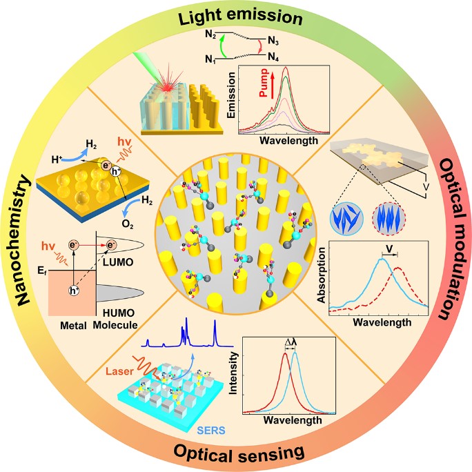
Molecular plasmonics, the area which deals with the interactions between surface plasmons and molecules, has
received enormous interest in fundamental research and found numerous technological applications. Plasmonic
metamaterials, which offer rich opportunities to control the light intensity, field polarization, and local
density of electromagnetic states on subwavelength scales, provide a versatile platform to enhance and tune
light-molecule interactions. A variety of applications, including spontaneous emission enhancement, optical
modulation, optical sensing, and photoactuated nanochemistry, have been reported by exploiting molecular
interactions with plasmonic metamaterials. In this paper, we provide a comprehensive overview of the
developments of molecular plasmonics with metamaterials. After a brief introduction to the optical
properties of plasmonic metamaterials and relevant fabrication approaches, we discuss light-molecule
interactions in plasmonic metamaterials in both weak and strong coupling regimes. We then highlight the
exploitation of molecules in metamaterials for applications ranging from emission control and optical
modulation to optical sensing. The role of hot carriers generated in metamaterials for nanochemistry
is also discussed. Perspectives on the future development of molecular plasmonics with metamaterials
conclude the review. The use of molecules in combination with designer metamaterials provides a rich
playground both to actively control metamaterials using molecular interactions and, in turn, to use
metamaterials to control molecular processes. As a versatile platform that can enhance and manipulate
optical phenomena on the nanoscale, plasmonic metamaterials will continue to advance molecular plasmonics
for the development of future photonic applications including ultrahigh-sensitivity optical sensing,
nanolasers, active functionalities, and photoactuated nanochemistry.
— P. Wang et al.,
Chem. Rev. 122, 15031–15081 (2022)
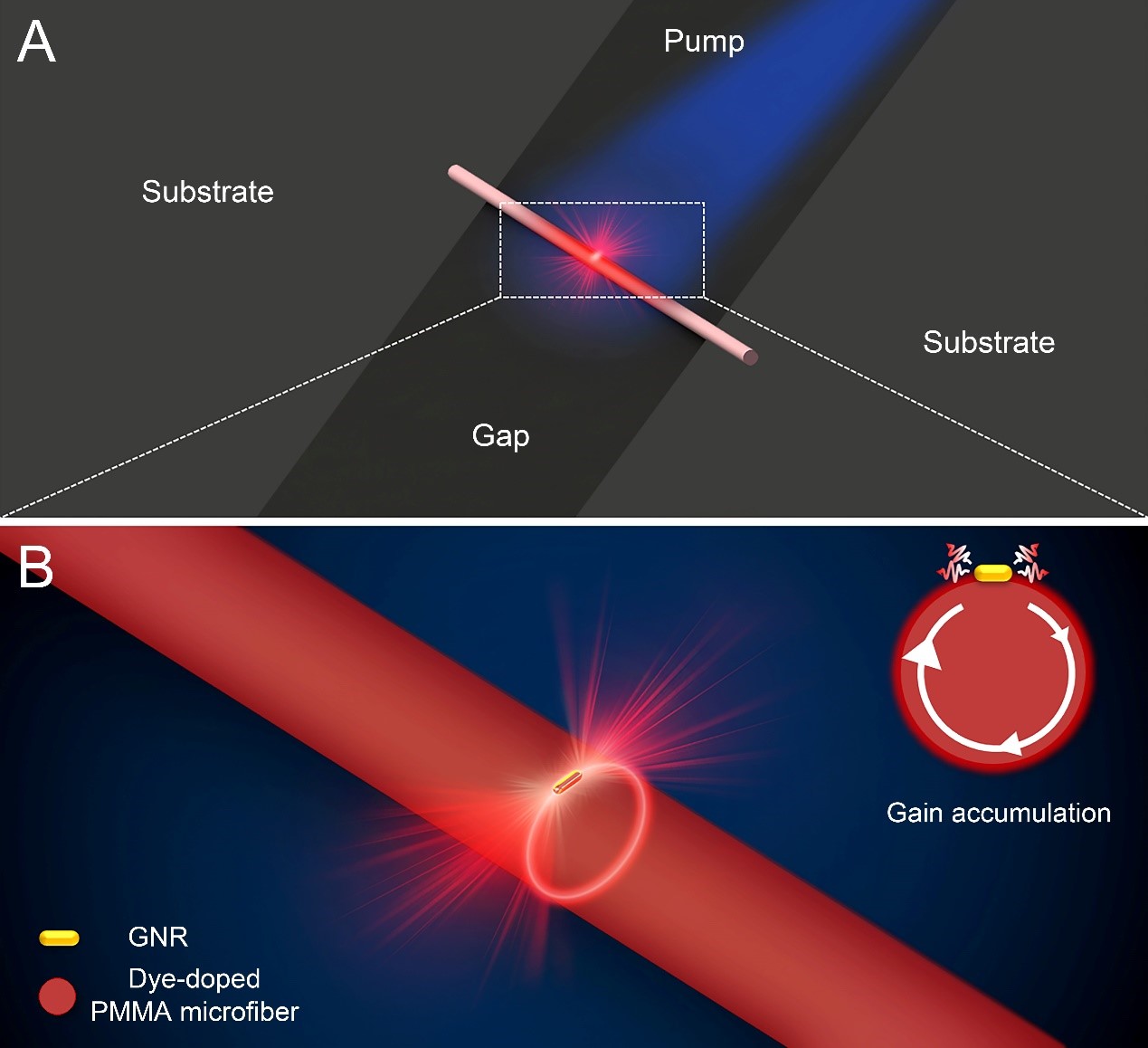
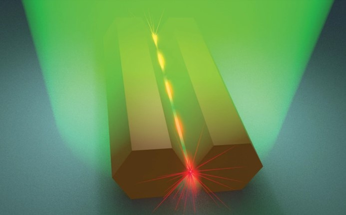
Laser based on single plasmonic nanoparticle can provide optical frequency radiation far beyond the
diffraction limit and is one of the ultimate goals of nanolasers, yet it remains a challenge to be realized
because of the inherently high Ohmic loss. Here, we report the direct observation of lasing in
microfiber-coupled single plasmonic nanoparticles enabled by strong mode coupling. We show that, by strongly
coupling a gold nanorod (GNR) with the whispering gallery cavity of a dye-doped polymer microfiber (with
diameter down to 2.0 μm), the substantially enhanced optical coherence of the hybrid photon-plasmon mode and
effective gain accumulated from the active microfiber cavity enable single-mode laser emission from the GNR at
room temperature with a threshold as low as 2.71 MW/cm2 and a linewidth narrower than 2 nm. The results
demonstrated here provide a feasible approach for the realization of lasers based on single plasmonic
nanoparticles and may find applications in areas such as ultraconfined field manipulation, ultrasensitive
sensing, and on-chip optical interconnects.
— N. Zhou et al.,
Sci. Adv. 8, eabn2026 (2022).
We proposed a photonic approach to a lasing mode supported by low-loss oscillation of polarized
bound electrons in an active nano-slit-waveguide cavity, which circumvents the confinement-loss
trade-off of nanoplasmonics, and offers an optical confinement down to sub-1-nm level with a
peak-to-background ratio of ~30 dB. Experimentally, the extremely confined lasing field is realized
as the dominant peak of a TE0-like lasing mode around 720-nm wavelength, in 1-nm-level width
slit-waveguide cavities in coupled CdSe nanowire pairs. The measured lasing characteristics agree
well with the theoretical calculations. Our results may pave a way towards new regions for
nanolasers and light-matter interaction.
— H. Wu et al.,
Phys. Rev. Lett. 129, 013902
(2022).
As a typical type of plasmonic nanostructures, nanoparticle-on-mirror nanocavity (NPoM), with the capability
of extreme optical confinement and enhancement, has triggered a series of breakthrough in nanophotonic
researches and applications. Here, we study the optical response of nanorod on mirror structure both
experimentally and theoretically. The strong coupling of a gold nanorod with an ultraflat single-crystalline
gold microflake produces rich and high-quality plasmonic modes related to complex interaction of film-coupled
nanorod modes and waveguide modes in the gap. Their optical responses are very sensitive to the thickness
(down to 15 nm) and refractive index of the dielectric spacer. Compared with the traditional nanocavity based
on thermally evaporated gold film, our nanocavity not only has stronger scattering intensity, but also has a
significant improvement in the quality factor of each mode. This low-loss NPoM nanocavity structure can also
integrate with fiber system efficiently and compactly. High-quality NPoM nanocavities are attractive for
studying light-matter interaction at the nanoscale, and promising for the construction of nanophotonic devices
such as nanolasers and plasmon-enhanced sensors.
— L. F. Liu et al.,
Nano Lett. 22, 1786-1794 (2022).
Strong coupling of a localized plasmonic mode to a low-loss photonic mode in a hybrid
plasmonic-photonic cavity provides a promising solution to elongate the LSPR lifetime via coherent
energy exchange and recirculation between the two otherwise uncoupled modes. Here, by placing a
single Au nanoparticle on the surface of a cadmium sulfide (CdS) nanowire, strong coupling of
localized surface plasmon resonance (LSPR) modes in the nanoparticle and whispering gallery modes
(WGMs) in the nanowire is demonstrated. For a 50-nm-diameter Au-nanosphere particle, strong coupling
occurs when the nanowire diameter is between 300 nm and 600 nm, with a mode splitting up to 80 meV.
Using a temperature-induced spectral shift of the resonance wavelength, the anti-crossing behavior
in the strongly coupled system is observed. In addition, since the Au nanosphere has spherical
symmetry, the supported LSPR mode can be selectively coupled with TE and TM WGMs in the nanowire.
The ultra-compact strong-coupling system shown here may provide a versatile platform for studying
hybrid “photon-plasmon” nanolasers, nonlinear optical devices and nanosensors.
— Y. Y. Jin et al.,
Nanophotonics 10, 2875-2881
(2021).
Ice is known to be a rigid and brittle crystal that fractures when deformed. We demonstrate that ice grown as
single-crystal ice microfibers (IMFs) with diameters ranging from 10 micrometers to less than 800 nanometers
is highly elastic. Under cryotemperature, we could reversibly bend the IMFs up to a maximum strain of 10.9%,
which approaches the theoretical elastic limit. We also observed a pressure-induced phase transition of ice
from Ih to II on the compressive side of sharply bent IMFs. The high optical quality allows for low-loss
optical waveguiding and whispering-gallery-mode resonance in our IMFs. The discovery of these flexible ice
fibers opens opportunities for exploring ice physics and ice-related technology on micro- and nanometer
scales.
— P. Z. Xu et al.,
Science 373, 187-192 (2021).
See also news and views in
1、E. M. Schulson, “Ice physics: A flexible and springy form of ice”, Science
373, 158 (2021).
2、浙江大学求是新闻网——用冰做光纤?浙大团队对冰的研究迈出一大步,成果登《科学》
3、浙大光电——浙大光电学院童利民教授团队研究成果在《Science》上发表
4、新华社——中美学者制备出可灵活弯曲的“冰光纤”
5、The New York Times —— A New Kind of Ice That Bends Like a Noodle Without
Breaking
6、New Scientist —— New kind of ice is so bendy it can curl
and uncurl without breaking
7、ScienceNews —— These weird, thin ice crystals are springy
and bendy
8、天目新闻——用冰制做光纤,浙大团队成果登《科学》
9、中国科学报——科学家用冰制备光纤并首次实现冰的弹性弯曲
10、科技日报——“冰光纤”问世,柔软且可高效导光
11、环球科学——我敢打赌,你从没见过这么弯的冰
12、DeepTech深科技——冰也有弹性!浙大团队成功生长高质量冰单晶微纳光纤,实现10.9%的弹性
应变 | 专访
13、Wissenschaft aktuell —— Elastische Fasern aus
Eis
14、NRC —— Perfect ijs breekt niet, maar buigt
15、GIZMODO —— This Bendable Ice Is Freaking Us Out
...

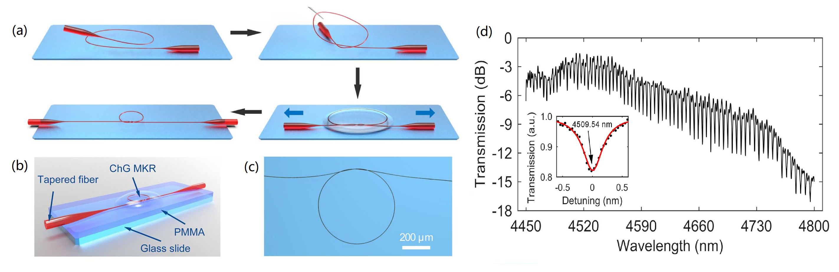
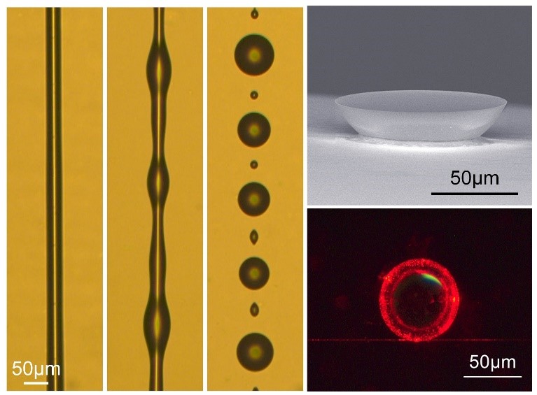
Optical microsphere resonators working in the near- to mid-infrared regions are highly required for a variety
of applications, such as optical sensors, filters, modulators and microlasers. Here, a simple and low-cost
approach for batch fabrication of high-quality chalcogenide glass (ChG) microspheres is demonstrated. By
melting high-purity ChG powders in a heated oil environment, As2S3 and As2Se3 microspheres with excellent
surface smoothness and extremely low eccentricity (~0.13%) can be readily fabricated. They exhibit excellent
resonant responses both in near- and mid-infrared spectral ranges (Q factor of ~106 around 1550 nm, and ~104
around 4.5 µm). The high-quality ChG microspheres demonstrated here are highly attractive for near- and
mid-infrared optics, including optical sensing, optical nonlinearity, cavity quantum electrodynamics,
microlasers, nanofocusing and microscopic imaging.
— Y. Xie et al.,
Small 17, 2100140
(2021).
Optical micro/nanofibers (MNFs) can be applied for ultrasensitive tactile sensing with fast response and
compact size, which are attractive for restoring tactile information in minimally invasive robotic surgery and
tissue palpation. Herein, we present a compact tactile sensor (CTS) with a diameter of 1.5 mm enabled by an
optical MNF. The CTS provides continuous readouts for high-fidelity transduction of touch and pressure stimuli
into interpretable optical signals, which permits instantaneous sensing of contact and pressure with
pressure-sensing sensitivity as high as 0.108 mN−1 and a resolution of 0.031 mN. Working in pressing mode, the
CTS can discriminate the difference between samples with shore a hardness of 36 and 40, a hardness resolving
ability even beyond the human hands. Benefitting from the fast response feature, the CTS can also be operated
in either scanning or tapping mode, making it feasible for hardness identification by analyzing the shape of
the response curve. Such MNF-enabled compact tactile sensors may pave the way for hardness sensing in tissue
palpation, surgical robotics, and object identification.
— Y. Tang et al.,
ACS
Appl. Mater. Interfaces 13, 4560-4566
(2021).
Wearable sensor is of vital importance for health monitoring, human-machine interaction and smart robot. In
order to monitor pressure or displacement with high sensitivity and fast response, we demonstrate a skin-like
wearable optical sensor (SLWOS) based on glass optical micro/nanofibers (MNFs) in thin layers of
polydimethylsiloxane (PDMS). Enabled by the transition from guided modes into radiation modes of the
waveguiding MNFs upon external stimuli, the skin-like optical sensors show ultrahigh sensitivity (1870
kPa-1), low detection limit (7 mPa) and fast response (10 μs) for pressure sensing, significantly
exceeding the performance metrics of state-of-the-art electronic skins. Electromagnetic interference
(EMI)-free detection of high-frequency vibrations, wrist pulse and human voice are realized. Moreover, a
five-sensor optical data glove and a 2×2-MNF tactile sensor are demonstrated. These initial results pave the
way toward a new category of optical devices ranging from ultrasensitive wearable sensors to optical skins.
— L. Zhang et al.,
Opto-Electron Adv. 3, 190022
(2020).
See also highlight in Opto-Electronic Advances
By integrating a free-standing cadmium sulfide (CdS) nanowire onto a silicon nitride (SiN) photonic chip, we
demonstrate a highly compact on-chip single-mode CdS nanowire laser. The mode selection is realized using a
Mach-Zehnder interferometer (MZI) structure. When the pumping intensity exceeds the lasing threshold of 4.9
kW/cm2, on-chip single-mode lasing at ~518.9 nm is achieved with a linewidth of 0.1 nm and a
side-mode suppression ratio of up to a factor of 20 (13 dB). The output of the nanowire laser is channelled
into an on-chip SiN waveguide with high efficiency (up to 58%) by evanescent coupling, and the directional
coupling ratio between the two output ports can be varied from 90 to 10% by predesigning the coupling length
of the SiN waveguide. Our results open new opportunities for both nanowire photonic devices and on-chip light
sources and may pave the way towards a new category of hybrid nanolasers for chip-integrated applications.
— Q. Y. Bao et al.,
Light-Sci. Appl. 9, 42 (2020).
See also highlight in Sensorexpert
Phys.ORG
EurekAlert!
Owing to their special merits including broadband transparency, high optical nonlinearity, and
hospitality to rare-earth dopants, chalcogenide glasses (ChGs) have been considered as highly promising
mid-infrared (mid-IR) photonic materials. Here, we demonstrate ChG microfiber knot resonators (MKRs) operating
in the mid-IR for the first time, and investigate the wavelength tunability, the structure of a PMMA-embedded
on-chip ChG MKR. ChG microfibers with typical diameters around 3 μm are taper-drawn from
As2S3 glass fibers and assembled into MKRs in liquid without surface damage. The
measured Q factor of a typical 824 μm diameter ChG MKR is about 2.84 × 10⁴ at the wavelength of
4469.14 nm. The free spectral range (FSR) of the MKR can be tuned from 2.0 nm (28.4 GHz) to 9.6 nm (135.9 GHz)
by tightening the knot structure in liquid. Benefitting from the high thermal expansion coefficient of
As2S3 glass, the MKR exhibits a thermal tuning rate of 110 pm • °C-1 at the
resonance peak. When embedded in polymethyl methacrylate (PMMA) film, a 551 μm diameter MKR retains a Q factor
of 1.1 × 10⁴. The ChG MKRs demonstrated here are highly promising for resonator-based optical
technologies and applications in the mid-IR spectral range.
— Y. Xie et al., Photonics Res. 8, 616-621
(2020).
In this study, SU-8 WGM microcavities are fabricated via a simple self-assembling method, with
smooth surface (σ
< 0.6 nm) and high Q factors (~104). The obtained microcavities show hemispherical shape, and can be
transferred onto arbitrary substrates with flat surfaces for characterizations and applications. As an
application of the microcavities, a sensitive temperature sensor is demonstrated by evanescently coupling a
SU-8 hemisphere with a silica microfiber. Owing to the package of polydimethylsiloxane (PDMS), the sensor
shows excellent long-term stability over one year with a sensitivity as high as 120 pm/°C in a range of
25-125°C. These results illustrate broad application potential of these simple fabricated polymer
microcavities in ultrasensitive sensors and microlasers.
— Z. Zhang et al., Nanoscale 11, 5203-5208 (2019).
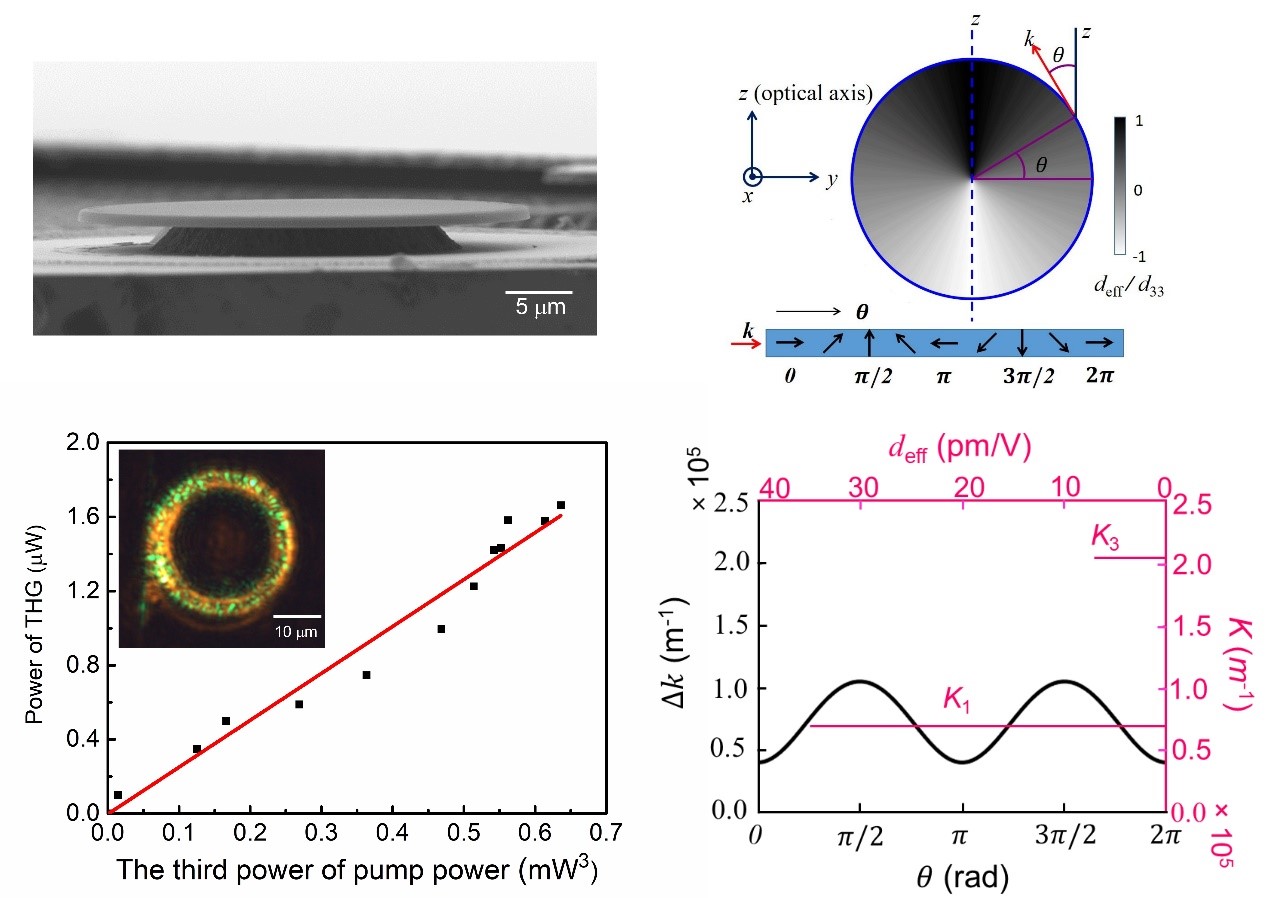
For light waves in the TE mode propagating along the circumference of a lithium niobate (LN)
microdisk, the effective nonlinear optical coefficients naturally oscillate periodically to change both the
sign and magnitude, facilitating natural quasi-phase matching (QPM) without the necessity of domain
engineering in the micrometer-scale LN disk. The second harmonic and cascaded third-harmonic waves are
simultaneously generated with normalized conversion efficiencies as high as 9.8% mW-1 and 1.05% mW-2,
respectively, thanks to the utilization of the highest nonlinear coefficient d33 of LN. The high efficiency
achieved with the microdisk of a radius of ~30 μm is beneficial for realizing high-density integration of
nonlinear photonic devices such as wavelength convertors and entangled photon sources.
— J. T. Lin, N. Yao et al., Phys. Rev. Lett. 122, 173903 (2019).
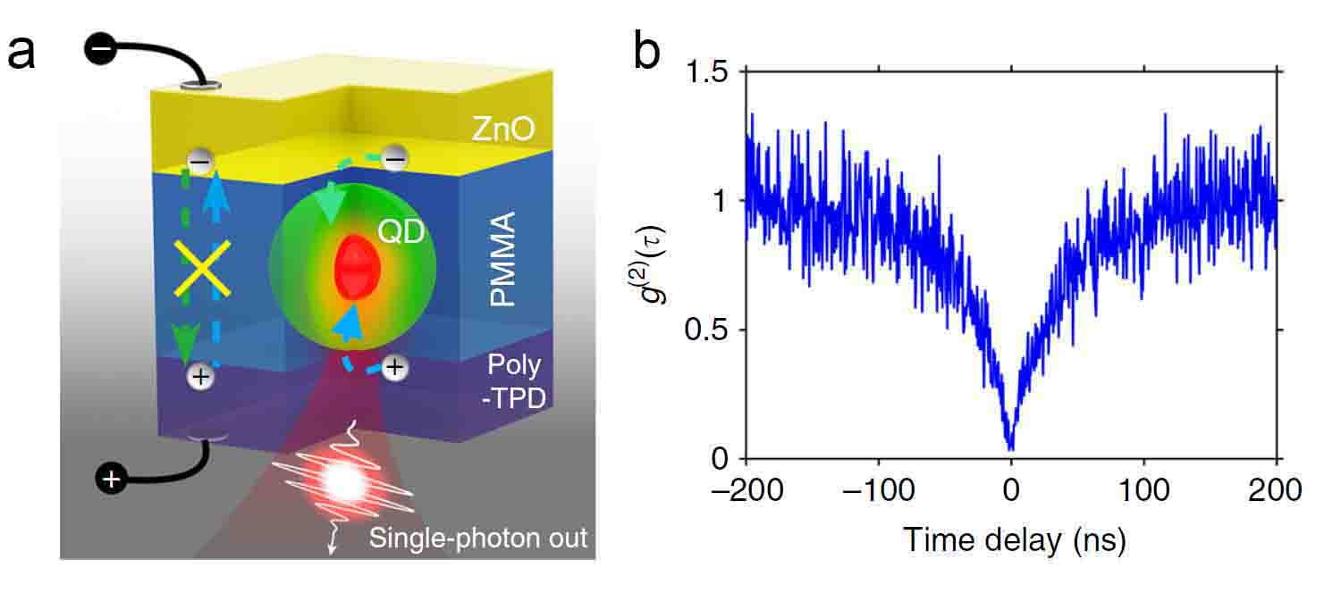
Photonic quantum information requires high-purity, easily-accessible, and scalable
single-photon sources. Here we report an electrically driven single-photon source based on colloidal quantum
dots. Our solution-processed devices consist of isolated CdSe/CdS core/shell quantum dots sparsely buried in
an insulating layer that is sandwiched between electron-transport and hole-transport layers. The devices
generate single photons with near-optimal antibunching at room temperature without any spectral filtering.
Such highly suppressed multi-photon-emission probability is attributed to both novel device design and carrier
injection/recombination dynamics.
— X. Lin et al., Nat. Commun. 8, 1132
(2017).
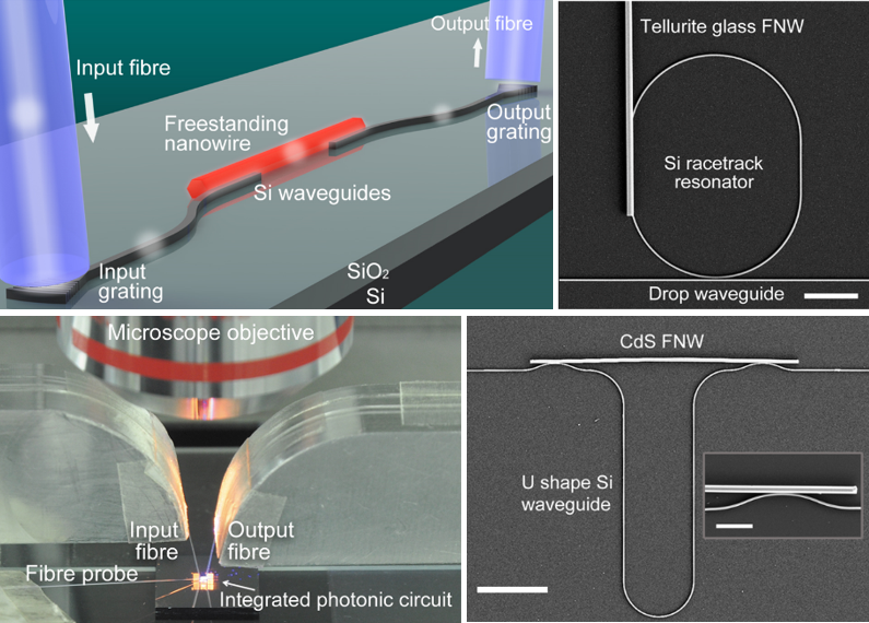
Silicon photonics has been developed successfully with a top-down fabrication technique to
enable large-scale photonic integrated circuits with high reproducibility, but is limited intrinsically by the
material capability for active or nonlinear applications. On the other hand, free-standing nanowires
synthesized via a bottom-up growth present great material diversity and structural uniformity, but precisely
assembling free-standing nanowires for on-demand photonic functionality remains a great challenge. Here we
report hybrid integration of free-standing nanowires into silicon photonics with high flexibility by coupling
free-standing nanowires onto target silicon waveguides that are simultaneously used for precise positioning.
Coupling efficiency between a free-standing nanowire and a silicon waveguide is up to ~97% in the
telecommunication band. A hybrid nonlinear-free-standing nanowires–silicon waveguides Mach–Zehnder
interferometer and a racetrack resonator for significantly enhanced optical modulation are experimentally
demonstrated, as well as hybrid active-free-standing nanowires–silicon waveguides circuits for light
generation. These results suggest an alternative approach to flexible multifunctional on-chip nanophotonic
devices.
— B. G. Chen et al., Nat. Commun. 8, 20
(2017).

Owing to their atomic layer thickness, strong light-material interaction, high nonlinearity,
broadband optical response, fast relaxation, controllable optoelectronic properties, and high compatibility
with other photonic structures, 2D materials, including graphene, transition metal dichalcogenides and black
phosphorus, have been attracting increasing attention for photonic
applications. By tuning the carrier density via electrical or optical means that modifies their physical
properties (e.g., Fermi level or nonlinear absorption), optical response of the 2D materials can be instantly
changed, making them versatile nanostructures for optical modulation. Here, up-to-date 2D materialbased
optical modulation in three categories is reviewed: free-space, fiberbased, and on-chip configurations. By
analysing cons and pros of different modulation approaches from material and mechanism aspects, the challenges
faced by using these materials for device applications are presented. In addition, thermal effects (e.g.,
laser induced damage) in 2D materials, which are critical to practical applications, are also discussed.
Finally, the outlook for future opportunities of these 2D materials for optical modulation is given.
— S. L. Yu et al., Adv. Mater. 29, 1606128
(2017).
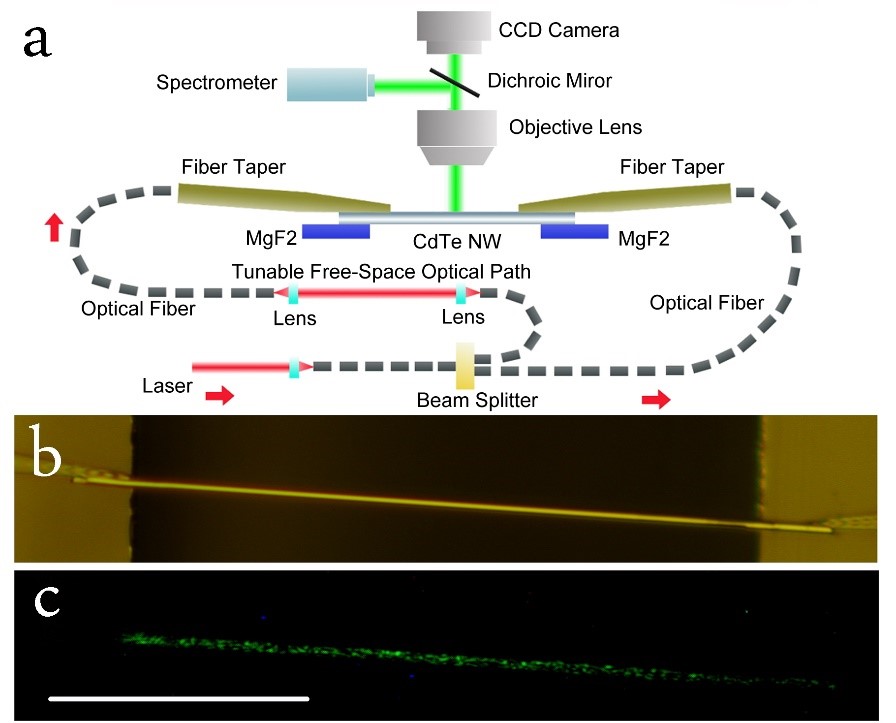
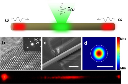
Relying on the transverse second harmonic (TSH) generation in a highly nonlinear CdTe nanowire,
we demonstrate a single nanowire optical correlator. Pulses to be measured were equally split and coupled into
two ends of a suspending nanowire via tapered optical fibers. By transferring the spatial intensity profile of
the TSH image into the time-domain temporal profile of the input pulses, we operate the nanowire as a
miniaturized optical correlator with input energy goes down to 2 fJ/pulse for 1064 nm 200 fs pulses. The
miniature fJ-pulse correlator may find applications from low power on-chip optical communication, biophotonics
to ultracompact laser spectroscopy.
— C. G. Xin et al., Nano Lett. 16, 4807-4810
(2016).
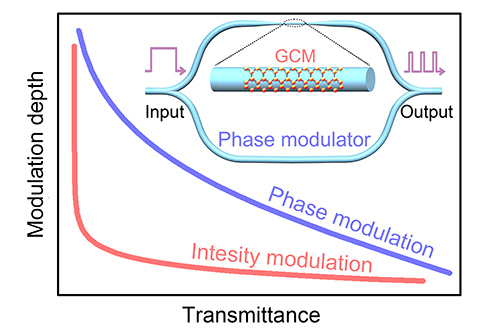
Graphene-based optical modulators have recently attracted much attention because of their
characteristic ultrafast and broadband response. Their modulation depth (MD) and overall transmittance (OT),
however, are often limited by optical loss arising from interband transitions. We report here an all-optical,
all-fiber optical modulator with a Mach-Zehnder interferometer structure that has significantly higher MD and
OT than graphene-based loss modulators. It is based on the idea of converting optically induced phase
modulation in the graphene-cladded arm of the interferometer to intensity modulation at the output of the
interferometer. The device has the potential to be integrable into a photonic system in real applications.
— S. L. Yu et al., Optica 3,
541-544 (2016).
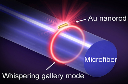
This paper reports a dramatic reduction in plasmon resonance line width of a single Au nanorod
by coupling it to a whispering gallery cavity of a silica microfiber. With fiber diameter below 6 μm, strong
coupling between the nanorod and the cavity occurs, leading to evident mode splitting and spectral narrowing.
Using a 1.46-μm-diameter microfiber, we obtained single-band 2-nm-line-width plasmon resonance in an Au
nanorod around a 655-nm-wavelength, with a quality factor up to 330 and extinction ratio of 30 dB. Compared to
an uncoupled Au nanorod, the strongly coupled nanorod offers a 30-fold enhancement in the peak intensity of
plasmonic resonant scattering.
— P. Wang et al., Nano Lett. 15, 7581–7586
(2015).
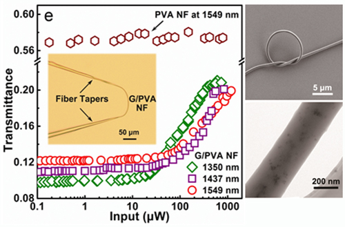
Graphene-doped polymer nanofibers are fabricated by taper drawing solvated polyvinyl alcohol
doped with liquid-phase exfoliated graphene flakes. As-drawn nanofibers, with typically diameter of hundreds
of nanometers and length up to tens of millimeters, show excellent uniformity and surface smoothness for
optical waveguiding. Owing to their tightly confined waveguiding behavior, light-matter interaction in these
subwavelength-diameter nanofibers is significantly enhanced. Using femto-second pulses around 1350-nm
wavelength, we demonstrate saturable absorption behaviors of such nanofibers with a saturation threshold down
to 0.25 pJ/pulse (peak power ~1.3 W). Additionally, using 1064-nm-wavelength naosecond pulses as switching
light, we show all-optical modulation of a 1550-nm-wavelength signal light guided along a single nanofiber
with switching peak power of ~3.2 W.
— C. Meng et al., Light: Science & Applications 4,
e348 (2015).
Integration of miniaturized elements has been a major driving force behind modern photonics.
Nanowires have emerged as potential building blocks for compact photonic circuits and devices in
nanophotonics. We demonstrate here a single nanowire optical correlator (SNOC) for ultrafast pulse
characterization based on imaging of the second harmonic (SH) generated from a cadmium sulfide (CdS) nanowire
by counterpropagating guided pulses. The SH spatial image can be readily converted to the temporal profile of
the pulses, and only an overall pulse energy of 8 μJ is needed to acquire a clear image of 200 fs pulses. Such
a correlator should be easily incorporated into a photonic circuit for future use of onchip ultrafast optical
technology.
— H. K. Yu et al., Nano Lett. 14, 3487-3490
(2014).
Graphene offers broadband light-matter interactions with ultrafast responses. The bandwidth of
previous graphene-based optical modulators were usually limited to ~1 GHz by electric parasite response. Now
by using an all-optical scheme, Li et al. show that a graphene-clad microfiber all-optical modulator can
achieve a modulation depth of 38% and a response time of ∼2.2 ps, corresponding to a bandwidth of ~200 GHz.
This modulator is compatible with current high-speed fiber-optic communication networks and may open the door
to meet future demand of ultrafast optical signal processing.
— W. Li et al., Nano Lett. 14, 955-959
(2014). ACS Editor's
Choice
In deep-subwavelength optical nanowires, the waveguiding loss increases with increasing optical
confinement, which may also lead to long-wavelength cutoff. Guo et al. pictured subtle balance between loss,
confinement and more in a recent article.
— X. Guo et al., Acc. Chem. Res. 47, 656-666
(2014).
By near-field coupling a CdSe and a Ag nanowires, Wu et al. demonstrated a hybrid
photon-plasmon laser operating at 723 nm wavelength at room temperature, which offers subdiffraction-limited
beam size and pure plasmon modes with mode area of 0.008λ2.
— X. Q. Wu et al., Nano Lett. 13, 5654-5659
(2013).
See also highlight in Phys.ORG
"Photon-plasmon nanowire laser offers new opportunities in light manipulation" by Lisa
Zyga
When a Au nanorod is placed inside an optical nanofiber, it can be efficiently excited by the
waveguiding mode with photon-to-plasmon conversion efficiency as high as 70%, and is highly potential for
realizing ultra-low power nanoparticle plasmonic devices. Check out more details of our Au-nanorod-doped
polymer nanofibers.
— P. Wang et al., Nano Lett. 12, 3145-3150
(2012).